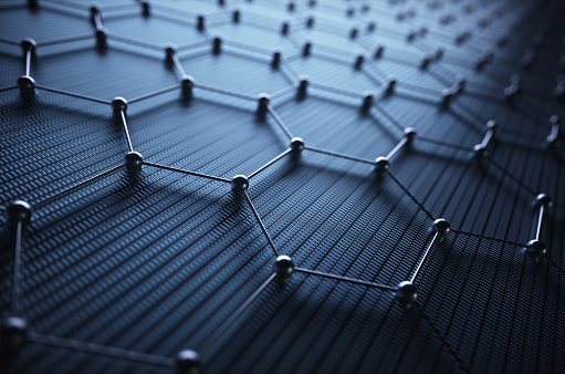
Unveiling the Potential of 2D Materials: Visualizing Embedded Interfaces
Scientists have made a breakthrough in the field of two-dimensional materials by developing a way to visualize the embedded interfaces between these materials and their two-dimensional environment. The new technique could help to improve the engineering of devices such as solar cells and transistors.
In a new paper published in Nature Communications, the team of researchers from the University of Cambridge and the University of Oxford describe their new technique that uses a combination of atomic force microscopy, Raman spectroscopy, and electron microscopy to visualize the embedded interfaces between two-dimensional materials and their two-dimensional environment. The technique allows scientists to observe how the interface between the two-dimensional material and its environment affects the properties of the material, such as its electrical conductivity and its ability to transport charge.
The findings provide a better understanding of how two-dimensional materials interact with their environment, which could lead to improved engineering of devices such as solar cells and transistors.
In a recent breakthrough, scientists from the University of Cambridge and the University of Oxford have developed a new technique to visualize embedded interfaces between two-dimensional materials and their environment. The technique, which combines atomic force microscopy, Raman spectroscopy, and electron microscopy, could help to improve the engineering
source: Phys.org